MAP33E1 SAS network topology error due to non-operational SES node
MAP33E1 Section-1
About this task
The FRU list of the serviceable event that sent you here contains:
- MAP33E1
- SAS cable (both ends)
- Enclosure services manager (ESM)
- RAID controller card or microbay
FRU location code formats are shown in Table 1:
| Component (FRU) | Location code (installed) | Location code, MES (uninstalled) | Figure reference |
|---|---|---|---|
| SAS cable, storage enclosure ESM end | U2107.D04.sssssss-P1-Cx-Ty | Rr-Fzz
-P1-Cx-Ty Fzz-P1-Cx-Ty |
Figure 1 |
| SAS cable, RAID controller end - microbay |
U1500.rBn.sssssss-P1-C7-Cx-Ty | Rr-Mzz-P1-Cx-Ty | Figure 2 |
| SAS cable, RAID controller end - device
adapter card, SAS (flash) |
U1500.rBn.sssssss-P1-Cx-Ty | Rr-XIn-P1-Cx-Ty | Figure 3 |
| SAS cable, RAID controller end - I/O enclosure (2U) adapter (PCIe and SAS device) |
U1600.iGn.sssssss-P1-Cx-Ty | iGn-P1-Cx-Ty | Figure 4 Figure 5 |
| Enclosure services manager (ESM) | U2107.D04.sssssss-P1-Cx | Rr-Fzz-P1-Cx Fzz-P1-Cx |
Figure 1 |
| Microbay |
U1500.rBn.sssssss-P1-C7-Cx | Rr-Mzz-P1-Cx | Figure 2 |
| Device adapter card, SAS (flash) | U1500.rBn.sssssss-P1-Cx | Rr-XIn-P1-Cx | Figure 3 |
| I/O enclosure (2U) adapter (PCIe and SAS device) |
U1600.iGn.sssssss-P1-Cx | iGn-P1-Cx | Figure 4 Figure 5 |
Procedure
Replace FRUs in the order listed in Table 1. Refer to the figures that follow for proper cabling. Point-to-point cabling diagrams are listed by model in Table 2.
Figure 1. Storage enclosure locations (rear view) (SAS flash enclosure, 24 drive slots)
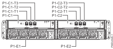
Figure 2. Flash SAS cable connectors - Microbay adapter card (Cx-T1, T2, T3, T4)
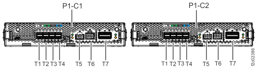
Figure 3. Flash SAS cable connectors - Device adapter card, SAS (flash) (Cx-T1, T2, T3, T4)
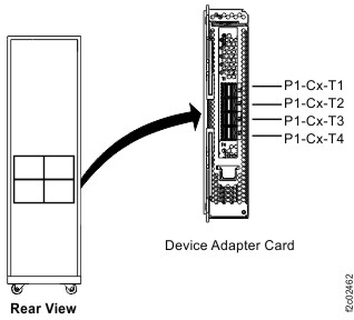
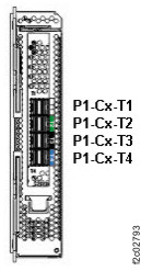
Figure 4. I/O enclosure (2U) (rear) (model 983)
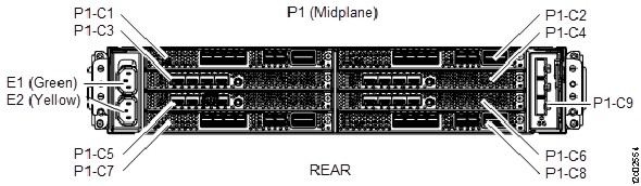
Figure 5. I/O enclosure (2U) adapter (PCIe and SAS device) (model 983)
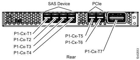
Figure 6. Point-to-point cabling diagram for storage enclosure flash SAS cables (Model 983, rear
view)
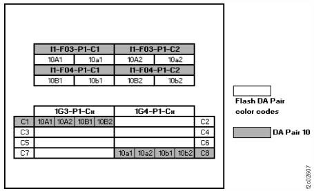
Figure 7. Point-to-point cabling diagram for storage enclosure FC-AL and Flash PCIe / SAS cables
(Models 984, 84E, rear view, racks 1, 2)
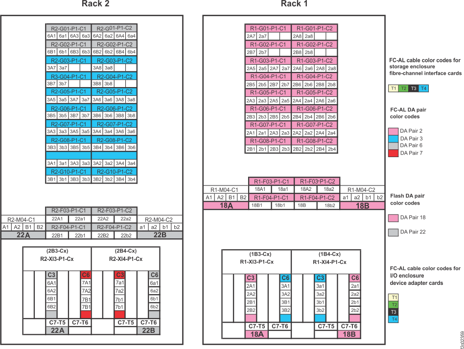
Figure 8. Point-to-point cabling diagram for storage enclosure Flash PCIe / SAS cables (Model 984
all-flash, rear view, rack 1)
Figure 9. Point-to-point cabling diagram for storage enclosure FC-AL and Flash PCIe / SAS cables
(Models 985, 85E, single-phase power, rear view, racks 1, 2)
Figure 10. Point-to-point cabling diagram for storage enclosure Flash PCIe / SAS cables (Models 985, 85E
all-flash, single-phase power, rear view, racks 1, 2)
Figure 11. Point-to-point cabling diagram for storage enclosure FC-AL and Flash PCIe / SAS cables
(Models 986, 86E, three-phase power, rear view, racks 1, 2)
Figure 12. Point-to-point cabling diagram for storage enclosure Flash PCIe / SAS cables (Models 986, 86E
all-flash, three-phase power, rear view, racks 1, 2)
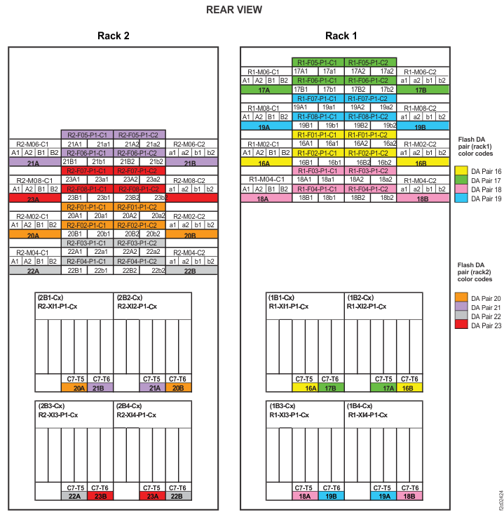
Figure 13. Point-to-point cabling diagram for storage enclosure Flash PCIe / SAS cables (Models 988,
88E, rear view, racks 1, 2)
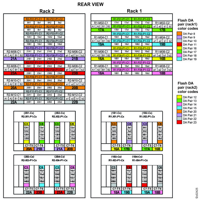
Figure 14. Point-to-point cabling diagram for storage enclosure Flash PCIe / SAS cables (Models 988,
88E, rear view, rack 3)
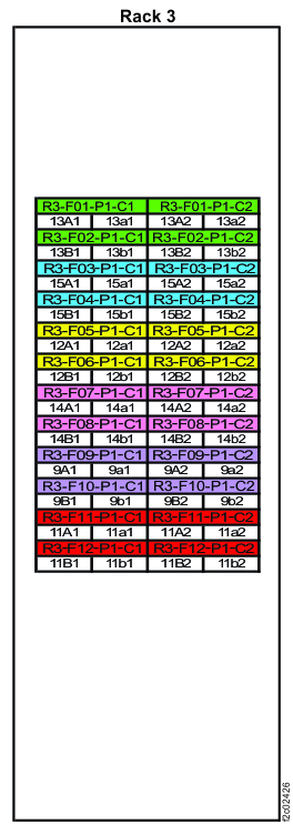
Figure 15. Point-to-point cabling diagram for storage enclosure Flash PCIe / SAS cables (Models 980, 98B
with HPFE Gen2) (rear view, racks 1 and 2)
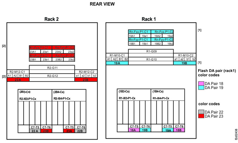
Figure 16. Point-to-point cabling diagram for storage enclosure Flash PCIe / SAS cables (Models 981, 98E
single-phase power with HPFE Gen2) (rear view, racks 1 and 2)
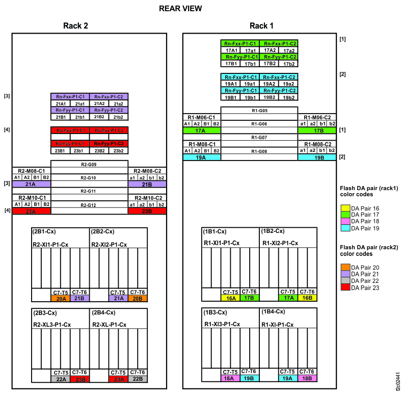
Figure 17. Point-to-point cabling diagram for storage enclosure Flash PCIe / SAS cables (Models 981, 98E
three-phase power with HPFE Gen2) (rear view, racks 1 and 2)
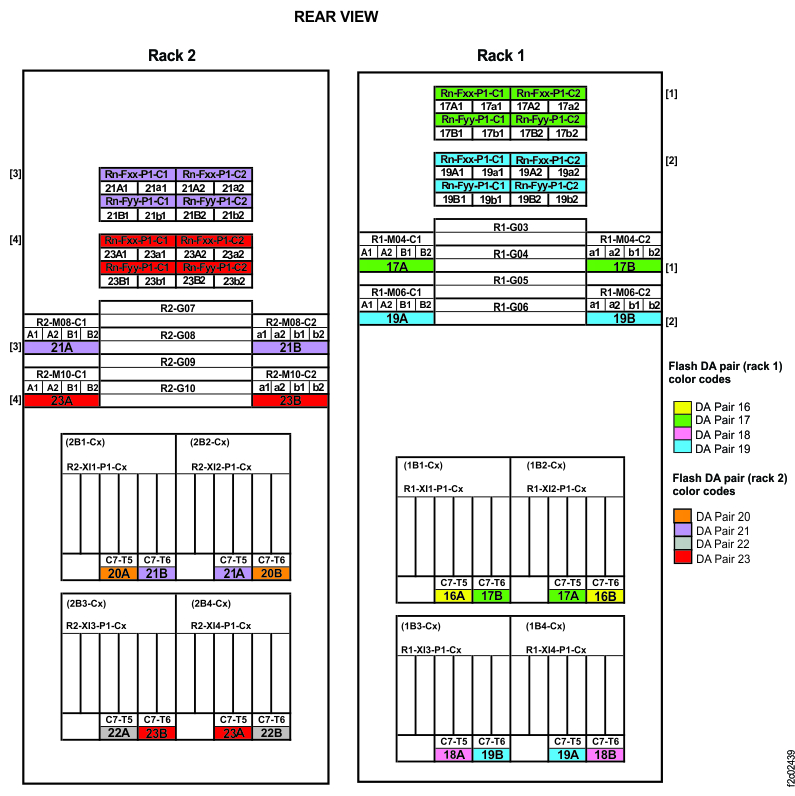
Figure 18. Point-to-point cabling diagram for storage enclosure Flash PCIe / SAS cables (Models 982, 98F
with HPFE Gen2) (rear view, racks 1 and 2)
If you were sent here by a storage enclosure installation, a
storage enclosure midplane repair, or an I/O enclosure midplane repair service action:
- Exit this MAP.
- To the question, "What was the result of using the service procedure? " click Delay the repair and then click Next.
- The current repair action ends, but the serviceable event that sent you here is left open. Close the serviceable event.
- Replace FRUs as necessary, beginning with the SAS cable.
- Restart the storage enclosure installation or midplane repair.
If you were sent here by a RAID controller or microbay repair action:
- Exit this MAP.
- To the question, "What was the result of using the service procedure? " click Delay the repair and then click Next.
- The current repair action ends, but the serviceable event that sent you here is left open. Close the serviceable event.
- The serviceable event associated with the original repair action should still be open and the RAID controller or microbay is not in a fully operational state. Restart the original repair action.
- When prompted to replace the FRU, replace FRUs as necessary, beginning with the SAS cable. If you replaced an ESM, you must pseudo-repair this ESM FRU after the repair of the RAID controller or microbay.
If you were sent here by an ESM repair action:
- The original ESM repair action has completed and any associated serviceable event associated with this action has been closed.
- Exit this MAP.
- Use the serviceable event that sent you here to replace FRUs, beginning with the SAS cable.
| For model: | Refer to this figure: |
|---|---|
| Models 980, 98B with HPFE Gen2 | Figure 15 |
| Models 981, 98E single-phase power with HPFE Gen2 | Figure 16 |
| Models 981, 98E three-phase power with HPFE Gen2 | Figure 17 |
| Models 982, 98F with HPFE Gen2 | Figure 18 |
| Model 983 | Figure 6 |
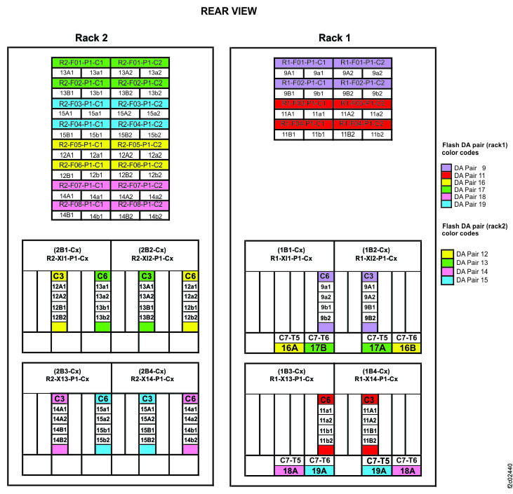
| Models 984, 84E | Figure 7 |
| Model 984 all-flash | Figure 8 |
| Models 985, 85E | Figure 9 |
| Models 985, 85E all-flash | Figure 10 |
| Models 986, 86E | Figure 11 |
| Models 986, 86E all-flash | Figure 12 |
| Model 988, Model 88E | Figure 13 Figure 14 |
Notes:
- Only HPFE Gen2 PCIe and SAS details are shown.
- For this model, physical locations are predefined for microbays, but not for HPFE Gen2 flash enclosures.
- The HPFE Gen2 enclosure pair can be located in a different rack than the associated microbay pair.
- The HPFE Gen2 enclosure locations are shown as Rn-Fxx (the upper enclosure of a pair) and Rn-Fyy (the lower enclosure of a pair).
Note: Only HPFE Gen2 PCIe and SAS details are shown.